Point: The LM555 timer remains a compact, versatile timing IC with supply ranges typically spanning low single-digit volts to mid-volt levels, timing from microseconds to minutes depending on R and C choices, and output drive capable of tens of milliamps—parameters that directly shape real designs.
Evidence: These ranges and limits are summarized in the official LM555 datasheet and represent the boundaries designers must translate into margins.
Explanation: This article turns those datasheet numbers into actionable design guidance so engineers can predict behavior, size components, and avoid common pitfalls when using the LM555 timer.
Point: Purpose-driven translation of datasheet detail saves prototype cycles.
Evidence: The goal here is to identify which specs matter, how to interpret guaranteed limits versus typical performance, and practical test steps.
Explanation: By focusing on supply, timing tolerances, output drive, and layout, designers get a clear checklist to validate timing circuits efficiently.
1 — LM555 timer: quick technical overview (background)
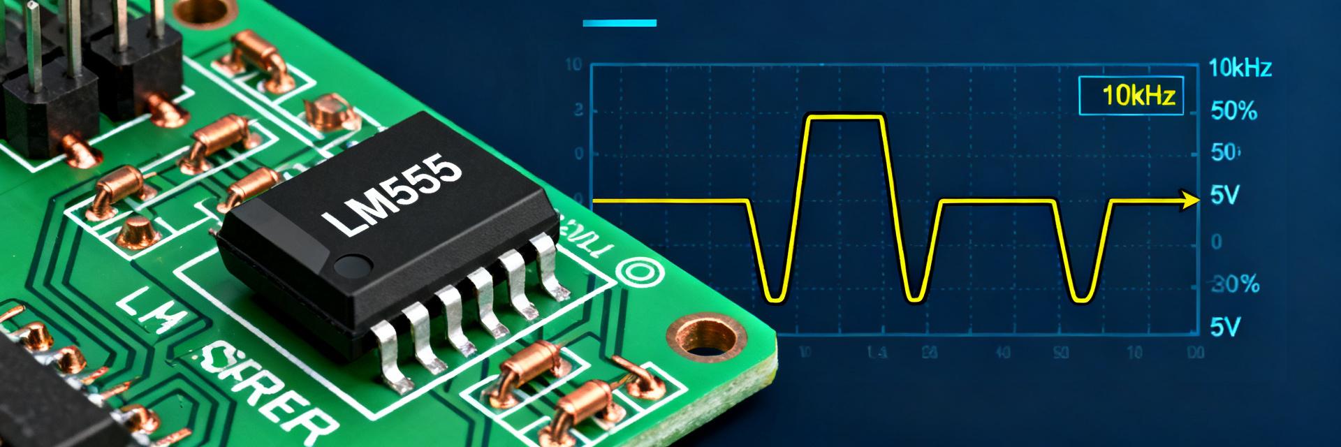
1.1 Pin functions & internal block summary
Point: The LM555 pinout includes VCC, GND, Threshold, Trigger, Output, Reset, Control Voltage, and Discharge; internally it pairs two comparators, an RS flip‑flop, a discharge transistor, and a push‑pull output stage.
Evidence: Datasheet block diagrams map each pin to specific blocks that set thresholds and switch the output.
Explanation: Actionable notes—never leave Threshold, Trigger, or Control Voltage floating; tie Reset high or through a defined resistor; place bypass caps at VCC/GND to stabilize comparator references and prevent false triggering.
1.2 Operating modes at a glance (monostable vs astable)
Point: Monostable mode yields a single pulse per trigger; astable mode produces continuous oscillation.
Evidence: Mode selection depends on how Threshold, Trigger, Discharge, and external R/C are connected.
Explanation: Choose monostable for pulse stretching and debouncing; choose astable for clocks, blinkers, or low‑frequency PWM. Practical tip: add a small cap on Control Voltage to reduce jitter in astable oscillators.
2 — Key electrical specs to read first in the LM555 datasheet (data analysis)
2.1 Supply voltage, supply current, and recommended operating conditions
Point: Extract VCC minimum/maximum, recommended operating range, quiescent current, and ambient temperature limits first.
Evidence: Datasheet lists absolute max and recommended VCC and quiescent ICC values under specified conditions.
Explanation: Use margins—design VCC well inside recommended range and budget quiescent current for battery applications; ambient temperature boundaries determine whether timing accuracy and current draw remain guaranteed.
| Specification Parameter | Bipolar LM555 (Standard) | CMOS LMC555 (Low Power) | Design Context & Margin Tip |
|---|---|---|---|
| Supply Voltage Range (VCC) | 4.5 V to 16 V (18 V Abs Max) | 1.5 V to 15 V (12 V typical) | Keep operating voltage ≥ 0.5V away from maximum limits. |
| Quiescent Supply Current (ICC) | 3 mA to 15 mA (VCC = 15V) | ~100 μA to 250 μA | Account for switching spikes in bipolar versions; use CMOS for low power. |
| Max Output Source / Sink | Up to 200 mA | 10 mA (Source) / 50 mA (Sink) | Bipolar drives relays directly; CMOS requires buffering. |
| Temperature Coefficient | 50 ppm/°C (Typical) | 150 ppm/°C (Typical) | Determine timing drift across operating range prior to PCB layout. |
2.2 Timing tolerances, thresholds, and temperature dependence
Point: Threshold and trigger levels are fractions of VCC (commonly 1/3 and 2/3) and the Control Voltage adjusts those references; timing depends on external R and C plus internal discharge switching.
Evidence: Datasheet shows typical vs guaranteed timing and how leakage/current through the timing capacitor and resistor tolerances affect period.
Explanation: To estimate worst‑case timing error, add resistor and capacitor tolerance percentage plus timing drift from temperature specs and capacitor leakage current influence into the calculation.
3 — Output stage and drive capabilities: what the datasheet reveals (data analysis)
3.1 Source/sink current, voltage swing, and load compatibility
Point: The LM555 output can source and sink tens of milliamps; voltage high/low levels shift under load.
Evidence: Datasheet tables list IO(source)/IO(sink) limits and VOUT high/low under specified loads.
Explanation: Actionable sizing—limit continuous loads to within datasheet currents, use a buffer or driver when interfacing with strict logic families, and account for VCC-dependent logic thresholds when connecting to other digital ICs.
3.2 Protection and dynamic behavior: short-circuit, thermal, and switching speed
Point: Datasheets indicate maximum continuous currents and typical rise/fall times; some variants include internal protection characteristics.
Evidence: Typical switching times and current limits help predict whether the device can drive LEDs, relays, or MOSFET gates directly.
Explanation: Bench tests—measure rise/fall and thermal behavior under expected loads; whenever in doubt, add a buffer transistor or MOSFET driver for inductive or heavy loads to protect the timer.
4 — Component selection & layout best practices for accurate timing (method guide)
4.1 Choosing R and C: formulas, tolerances, and practical examples
Point: Standard formulas—monostable pulse width T = 1.1·R·C; astable frequency f ≈ 1.44/((RA+2·RB)·C).
Evidence: These formulas come from the internal charge/discharge timing behavior described in the datasheet.
Explanation: Worked examples—target 1 ms: pick R=10 kΩ and C≈0.1 μF (T≈1.1·10k·0.1μF=1.1 ms); target 1 s: use R≈910 kΩ and C≈1 μF. Account for resistor ±1% vs ±5% and capacitor tolerance/leakage when estimating worst‑case timing. Long‑tail searches to use: "LM555 timer calculation", "555 timing capacitor selection".
4.2 Power supply decoupling, grounding, and PCB layout tips
Point: Decoupling near VCC/GND pins and short return paths reduce jitter.
Evidence: Datasheet recommends bypass capacitors and shows sensitivity to supply transients.
Explanation: Use a 0.1 μF ceramic at the VCC pin, a 10 μF bulk cap nearby, keep traces short, route ground plane beneath the IC, and avoid routing noisy signals near timing components. Checklist: prototype with short wires and then tighten layout for production.
5 — Common pitfalls, diagnostics, and troubleshooting checklist (method guide)
5.1 Typical failure modes and their datasheet origins
Point: Symptoms like unstable frequency, missed triggers, or stuck outputs tie back to floating pins, supply sag, or capacitor leakage.
Evidence: Datasheet specs reveal sensitivity to control voltage and supply variations.
Explanation: Inspect Control Voltage for noise, verify Reset is asserted appropriately, and replace suspect capacitors with low‑leakage types to resolve drift issues.
5.2 Quick troubleshooting flowchart for lab debugging
Point: Orderly checks accelerate fault isolation.
Evidence: Practical lab experience maps common faults to simple tests.
Explanation: Follow this sequence—(1) verify VCC/GND and decoupling, (2) check Reset and Control Voltage levels, (3) observe Trigger/Threshold on scope, (4) remove load to test output, (5) substitute timing capacitor or IC if uncertain.
6 — Practical example circuits and selection checklist before adoption (case/action)
6.1 Two concise example builds (astable oscillator, monostable pulse generator)
Point: Concrete builds validate theory.
Evidence: For an astable 1 kHz LED flasher, choose RA=10 kΩ, RB=10 kΩ, C=0.01 μF yielding f≈1.44/((10k+2·10k)·0.01μF)≈1 kHz; for a monostable 100 ms pulse, choose R=91 kΩ and C=1 μF (T≈100 ms).
Explanation: Expect tolerances from resistor and capacitor specs; verify with scope at test points: output, threshold, and discharge node.
6.2 Final selection & pre-production checklist (will it meet your spec?)
Point: Confirm key datasheet items before commitment.
Evidence: Datasheet entries to verify include VCC range, quiescent current, max sink/source current, timing error bounds, temperature rating, and package thermal limits.
Explanation: Run prototype tests at worst-case VCC and temperature extremes, validate timing against the official LM555 datasheet guarantees, and plan buffering if loads approach IO limits. Note: LM555M can appear in part codes—verify the exact variant for thermal and current specs.
Summary / Conclusion
Point: The most critical datasheet items for reliable LM555 timer use are supply limits, timing accuracy with temperature and component tolerances, output drive capability, and layout/decoupling practices.
Evidence: Each of these items appears as guaranteed limits or recommended practices in the official LM555 datasheet and directly impacts real‑world performance.
Explanation: Validate timing in prototype under worst‑case voltage and temperature, use low‑leakage capacitors for long pulses, and add buffering for heavy loads. Also confirm variant‑specific limits—some suffixes (e.g., LM555M) denote package or thermal differences that matter in production.
- Check VCC and quiescent current against your supply budget and operating temperature to ensure reliable operation with the LM555 timer.
- Estimate worst‑case timing by combining resistor/capacitor tolerances with capacitor leakage and datasheet timing drift values.
- Confirm output source/sink limits and add a buffer for inductive or high‑current loads to protect the timer.
- Apply local decoupling (0.1 μF + 10 μF), short ground returns, and keep timing components close to the IC for minimal jitter.
FAQ
How accurate is the LM555 timer for precise timing applications?
Typical accuracy depends on resistor and capacitor tolerances plus temperature drift specified in the datasheet. For high precision, use 0.1% resistors, C0G/NP0 capacitors with low leakage, and stabilize Control Voltage; always verify worst‑case error by summing component tolerances and datasheet timing drift.
Can the LM555 timer directly drive LEDs or relays?
The LM555 can source/sink tens of milliamps suitable for LEDs (use current‑limiting resistors), but driving relays or heavy inductive loads typically requires a driver or transistor stage to avoid exceeding IO limits and to protect against inductive kick.
What tests should I run on a prototype to validate LM555 timing?
Measure VCC under load, verify Reset and Control Voltage levels, capture timing waveforms at Output and Discharge with an oscilloscope across supply and temperature extremes, and swap capacitors to check for leakage effects. These steps confirm operation versus the LM555 datasheet guarantees.
What is the difference between standard bipolar LM555 and CMOS versions like LMC555?
Bipolar LM555 devices support wider supply voltages and higher drive currents but draw significant supply current spikes during switching. CMOS variants like the LMC555 draw vastly less quiescent current and minimize supply transients, making them ideal for low-power battery-operated designs despite lower output drive limits.


